

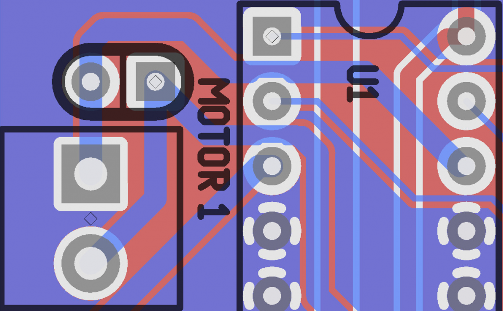
Click for larger image
As you may notice near the center of the image I passed the outputs from the far side of the chip between two pins. Increasing the trace thickness as the traces were originally drawn caused some DRC (Design Rule Checker) issues. I replaced the trace between the pins with sections to let me increase the size of specific parts of the trace leaving notches where the traces pass by the pins. Am I askng for trouble? For higher power applications, would it be better to suggest to those wishing to, to scrape off the solder mask over those lines and add solder to give higher current handling capacity? Am I making much ado about nothing with respect to the target audience of this board?