Hello Kakwu
Thanks a lot for the question. Before giving out the answer I have a certain questions on my mind, which I have to know at first before giving the answer,
As long as you are driving the device with a pulse signal at about 1 kHz or higher, with a duty cycle between say 2% and 98%, the bootstrap circuit should work.
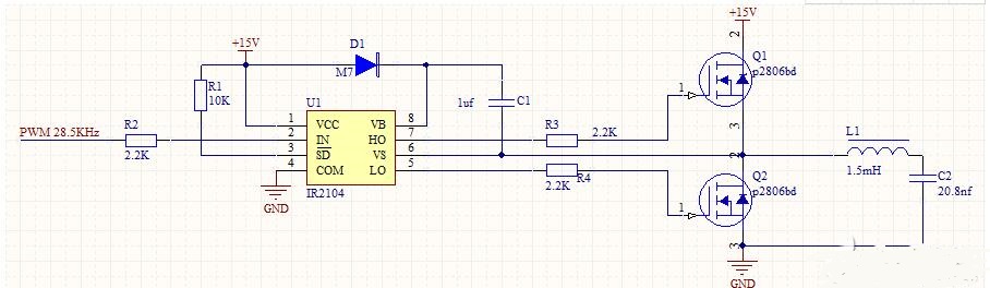
Check that your circuit matches the design in the datasheet. In particular, check that you have:
(a) a suitable diode between VCC (pin 1) and VB (pin 8);
(b) a capacitor between VB (pin 8) and VS (pin 6);
(c) a connection from VS (pin 6) and the MOSFETs.
Measure the DC voltage between VB and VS (pins 8 and 6). It should be slightly less than VCC.
If you haven’t solved the problem, please tell us:
(1) What is the frequency of your driving signal?
(2) What are the minimum and maximum duty cycles of your driving signal?
(3) What is your VCC voltage?
(4) What is the part number of the diode from VCC to VB?
(5) What value capacitor are you using between VB and VS?
Basically, the main thing on this are
The capacitor charges through the diode when the bottom MOSFET is conducting, and discharges into the VB pin when the top MOSFET is conducting. You don’t need to charge it manually yourself. This happens automatically while the driver is switching.
The whole circuit needs to be fully connected in order for the top MOSFET to switch. If you have disconnected part of the circuit for testing, this may prevent the driver IC from generating the gate drive voltage for the top MOSFET.
What is the supply voltage on the drain of the top MOSFET? Is that fed from your main 12V supply as well?
Please install a 1 uF component for the bootstrap capacitor, and measure the voltage across it, with the drive signal present and the MOSFETs fully connected.
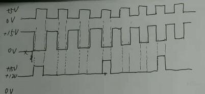
Also if you have an oscilloscope, look at the drive signals on the LO and HO outputs (pins 5 and 7). The LO signal (pin 5) should be a 50 Hz, 50% duty cycle square wave that swings from 0V to 10~12V. The HO signal (pin 7) should be a 50 Hz. 50% duty cycle square wave that swings from 0V to some higher voltage, about 10~12V higher than the voltage on the drain of the top MOSFET.
If those signals are not as I described, please describe the waveforms and the minimum and maximum voltages on those two pins.