

MaxBoard-rev2.zip (78346Bytes)
9-29-2014: This update just adds the zip file containing the board in its current layout. Send the zip file to your favorite board house and get your own stack of boards. :) I still have a few that I am dispersing.
A week or so ago Max was trying to find a layout for a PICAXE 18 or 20 board with an L293/754410 motor driver. He was hoping for something similar to what sanc04 assembled.
After spending some time with my layout software of choice, I had to walk away for a bit because the group that works on the schematic software and the group that works on the pcb software do not communicate very well. :P What I am saying is not all of the symbols and footprints jive with respect to their pin labels. It causes connections in the pcb software to be misrouted.
Before I got hip deep in laying out the board, I hit up some of the more intelligent minds in the SB to get an opinion on my schematic. First, I am sorry I don't recall everyone that was offering advice on the board. I remember bdk6 specifically because I know he is on top of the layout/schematic/design game. :) bdk6 suggested 3 extra capacitors and jumpers to allow for use of external power for the 3 pin headers attached to Port B. He also suggested that the option be split between the 8 connections half and half.
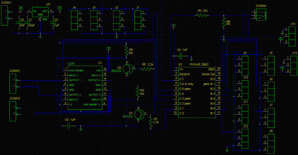
What you see above is what I came up with. I did make a few adjustments after I started laying it out in the pcb software, but, nothing too terribly important.
A week or so after games in Windows I jumped back on Max’s board. I managed to get my symbols and footprints straightened out and moved on to actually laying out the board.
Knowing that the board might be sent off to be produced, I was hoping I could get it to fit in the 2" x 2" area that the board houses charge the least for. Success! (i think)

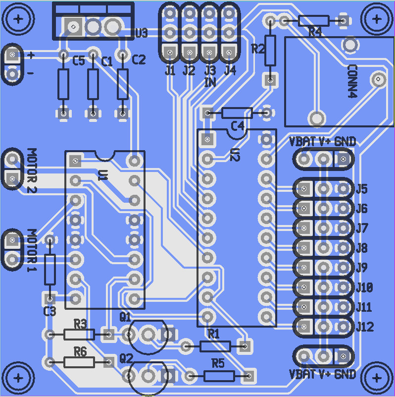
The above image can be clicked for a full size image.
I am showing this off here to hopefully get some input as to whether or not this is a viable layout. I see no reason in wasting a board house’s time to have someone tell me this board just ain’t gonna cut it. (In case anyone is curious. The circles in the corners are meant to be 3mm mounting holes.)
If the above board is viable, I may consider trying to make one myself first just to see if I can.
Side note: I use gEDA and PCB for my schematics and pcb layout.
6-28-2013 Updates
sanc04 pointed out a DOH! error on my part. The board above would work, but, the motordriver would need to be inserted backwards in to the board. Not a good plan 
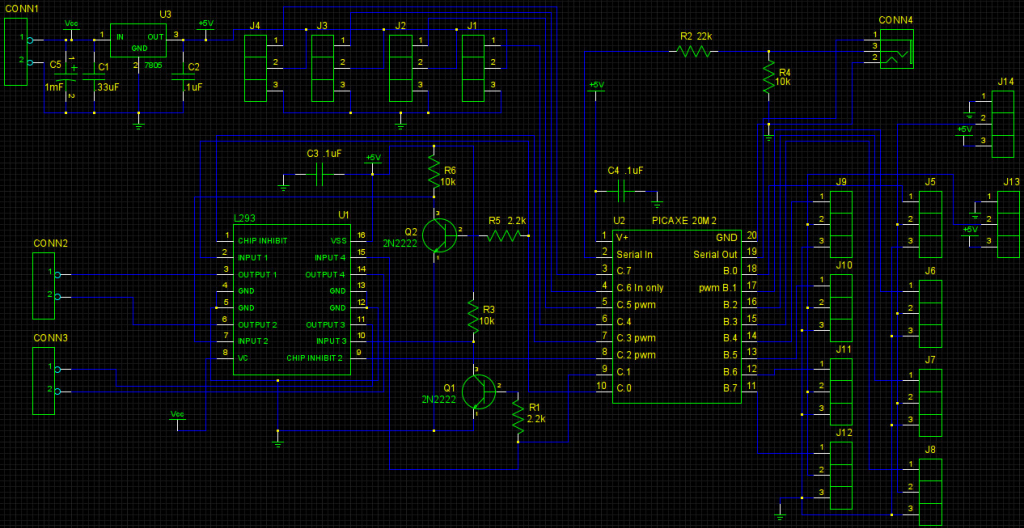
Updated schematic (Click to view full sized)

Basically just moved a few traces and C3.
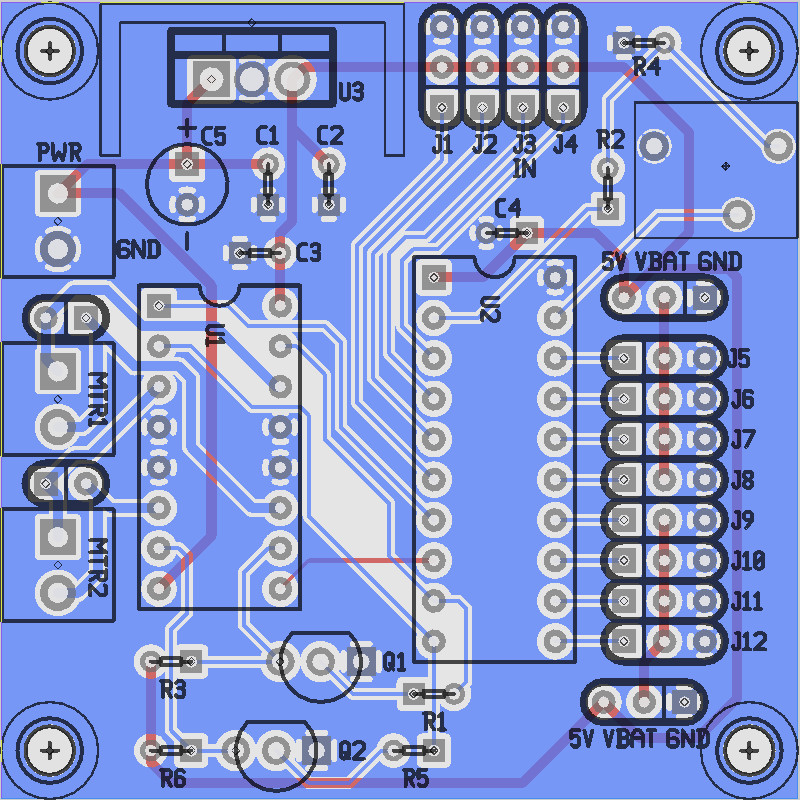
Updated board (Click to open full size)

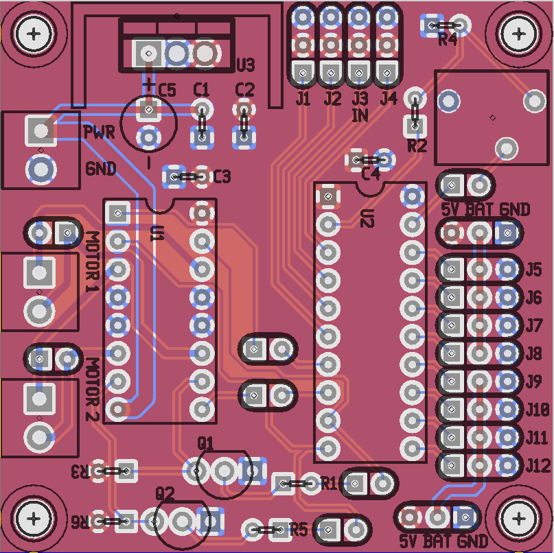
Added inexpensive heatsink, screw terminals, changed the stereo jack to one from Jameco, added more spacing due to outline of screw heads. All of the resistors were changed from laying down to standing up, hence the .1" spacing. The screw terminals for the motors are optional. If they aren’t installed, the labels will be visible. After a bit of finagling, I believe it will pass OSHPark DRC. There are a few bits that are pushing the limits. Namely the 4 3 pin headers at the top and the stereo jack at the edge of the board.
I didn’t manage to save myself any area (poor knowledge of layout?). I did, however, get by with less copper being etched.
Any more suggestions before I actually try to have this made?
Max says there are a number of people that would want these, if they are producable. I will throw up a parts list with an attempt to source everything from Jameco for no better reason than that is where I located a couple of the components I drew up to include (heatsink, stereo jack). The holes are 3mm w/ silkscreen for 6mm heads.
| U1 | L293DNE | $2.95 | Jameco PN 1341966 | ||
| U2 | PICAXE 20X2 / PICAXE 20M2 | $3.20 | RobotShop PN RB-Pic-31 | ||
| U3 | 7805 | $0.29 | Jameco PN 51262 | ||
| (optional) | 2940 | $1.55 | Jameco PN 897381 | ||
| Heatsink | $0.29 | Jameco PN 326596 | |||
| R1, R5 | 2.2k 1/4W (minimum purchase 10) | $0.99 | Jameco PN 690945 | ||
| R2 | 22k 1/4W (minimum purchase 10) | $0.99 | Jameco PN 691180 | ||
| R3, R4, R6 | 10k 1/4W (minimum purchase 10) | $0.99 | Jameco PN 691104 | ||
| C1 | .33 uF | $0.32 | Jameco PN 33523 | ||
| C2 – C4 | .1 uF | $1.17 | Jameco PN 33488 | ||
| C5 | 1000 uF | $0.25 | Jameco PN 30015 | ||
| Q1, Q2 | 2N2222 (minimum purchase 10) | $0.70 | Jameco PN 178512 | ||
| CONN 1 | Screw terminal | $0.39 | Jameco PN 2094506 | ||
| CONN 2, 3 | 2 x 2 pin headers | ||||
| (optional) | Screw terminals | $0.78 | Jameco PN 2094506 | ||
| CONN 4 | Stereo Jack | $1.49 | Jameco PN 2095437 | ||
| DIP 16 socket | (minimum purchase 10) | $2.00 | Jameco PN 112222 | ||
| (optional) | $0.75 | Jameco PN 37402 | |||
| DIP 20 socket | (minimum purchase 10) | $1.70 | Jameco PN 112248 | ||
| (optional) | $0.85 | Jameco PN 38623 | |||
| Headers | 2 x 40 position header strips | $1.50 | Jameco PN 160882 | ||
| Base total No options No PICAXE | $16.02 | ||||
| All Options No PICAXE | $15.96 |
No shipping costs are included in the above Parts list. I would imagine most of the parts are already in ones parts bins. The transistors could be swapped for 2n3904s, I believe. I am sure the smart people around here can suggest capacitor ranges. I am sure you can mix and match parts to come in under $16 + PICAXE, board, and shipping. I just checked Jameco shipping. I managed to get the price to $14.73 + $7.90 shipping.
One thing I am extremely concerned about is whether or not I read the drawing correctly for the stereo jack. I don’t imagine the jack can be plugged in to the other side of the board. Either that or I just got the dimensions all kinds of wrong, and, it will be more like a square peg in a round hole.
07-03-2013 UPDATE
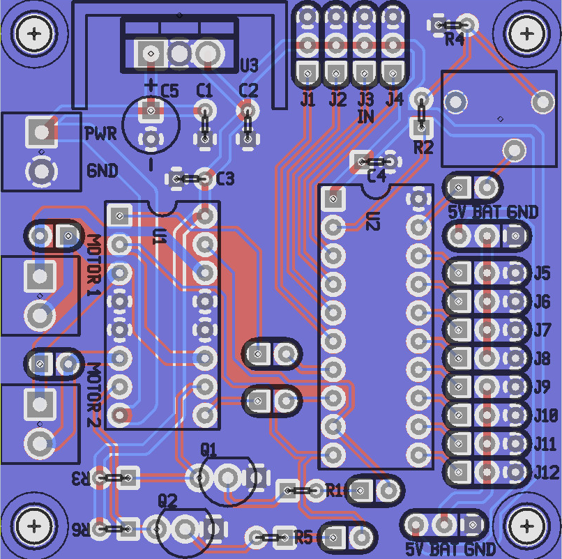
After deciding to go to a double sided board and talking to Dan M, I spun some mods into the original plan.

Click image for full size version
I added jumpers on the 4 lines that were originally hardwired to the motor driver. A jumper was installed between the stereo jack and the Serial Out pin. I increased the thickness of the line that goes to the motor driver. Also, obviously, I made the top layer a power plane to cut down on some of the power runs.
I welcome any comments. I would like critiques on anything anyone thinks should be changed or modified.
It seems the top layer being 5V is a phenominally bad idea.  There was mention of the makings of a plate capacitor. Worse yet MarkusB offered that a small scratch in the solder mask under the heatsink could be really bad too.
There were more calls for a shield like setup. Either way I will have to do a bit of rerouting. I will update this in a few days.
Ok, I lied. After a nap I converted the top layer to a second ground plane, and, increased the thickness of the traces that feed the motors.

Click for larger image
Update 9-25-2013
I made a mess of things not once, but, twice. The artwork above has two major issues and a minor one.
- The footprints for all of the headers are SIP footprints. SIP pins are the size of IC pins and not the nearly 1mm required to allow the headers to fit.
- The footprint for the stereo jack has holes that are about 1/3 the size they need to be.
- The footprint I used for the “big” electrolytic at the Vreg was too small when compared to the actual capacitor I have.

Click image for larger version
All of that means that the beautiful, purple OSHPark boards I have, won’t work. At all.
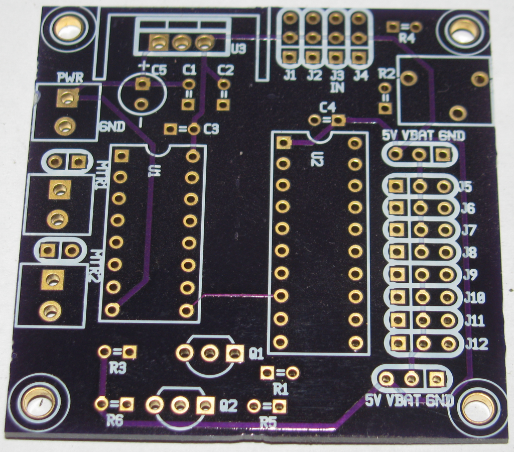
Skip ahead a month, or, back a few days ago based on the date of this update. I received my next set of boards from SeeedStudio after first forgetting to add an outline, then not making a completely closed outline. Doh!

Click image for larger version
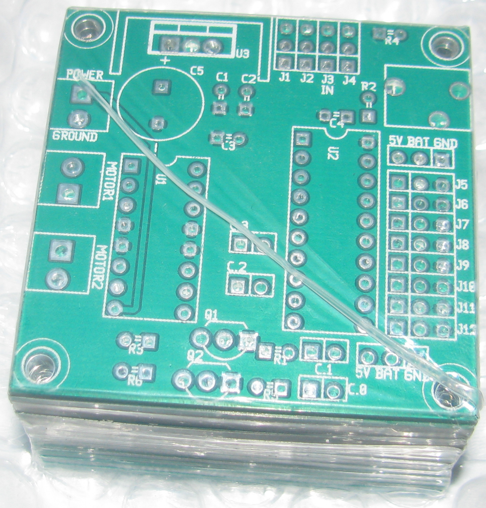
Mail comes and a box with a stack of pretty green boards from Seeed. I start looking them over. Test fitting a few parts. Then I look at the bottom side. It is solid green. Where are the traces, I think to myself. Maybe they are hidden under the soldermask. Out comes the DVM. No conectivity between pins. WTH?!?
I go back and look at the artwork I sent them. The gerber layer labeled bottom by gEDA is not the same type of layer as the one labeled top. The top layer is what you would expect with all the connections that one has made on the top layer of their board. The one labeled bottom is only the annular rings. There are no traces. Looking at a different form of export I found that the layer labeled group1 is the layer I needed to include and label as the bottom layer.
So, I have updated some things. I increased the size of most all of the annular rings. I was not happy with their size on my second set of unusable boards. Increasing their size required me to shrink the size of the motor leads where it passes between the motor driver pins. The new boards were ordered( re-ordered ) today. I will see if I can get Max’ board to him before he dies of old age.
Only bonus to all this messing is that I am learning what mistakes to not make again.
Dropbox link to the ps file for anyone that wants to try printing one of these at home. I am not sure how easy it would be. there are some 10 mil traces. The only reason it is double sided is to let me run power from the input to the motors.